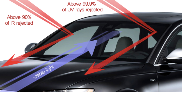
By blending sputtered layer with layer of ultra nano ceramic carbon with an ideal balance, IRIS V90 blocks solar heat, IR, UV rays and such with the best performances and provides nice interiors.
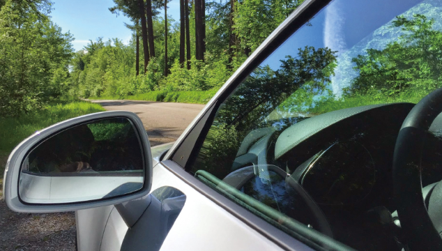
Exceptionally Clear View
Exceptionally clear views by using PET and carbon layers with high transparency and allowing effective visual light transmission.
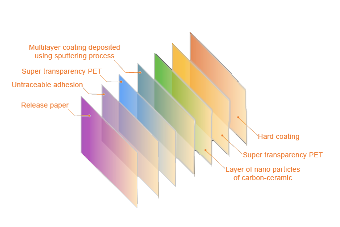
Multi-layer sputtering is a process of depositing thin films of different materials onto a substrate in layers using a sputtering technique. Sputtering is a physical vapor deposition (PVD) process where atoms of a target material are ejected from a surface through ion bombardment and deposited onto a substrate.
With multiple targets in use, each consisting of a different material, and careful control of the deposition parameters like the thickness of each layer, the resulting film can have unique properties for different applications. Multi-layer sputtering is widely used in the production of semiconductor devices, solar cells, and optics.
In semiconductor manufacturing, multi-layer sputtering can be used to build different layers of the metallization process, which is the process where the lines and vias that connect different parts of the semiconductor device are created. The technique also has applications in the production of charge-coupled devices (CCDs), photovoltaic cells, and flat-panel displays.
Sputtering technology of special alloy and nano ceramic fusion technology, has the greatest heat reflective performances and perfectly blocks UV rays, IR and such while allowing efficient visual light transmission. Thereby, the film creates nice driving conditions anywhere and at any time.